News

New eBook from Mouser Electronics and NXP Semiconductors offers insights into design challenges for vehicle electrification

Mouser Electronics, Inc., the industry’s leading New Product Introduction (NPI) distributor with the widest selection of semiconductors and electronic components™, launched a new eBook in collaboration with NXP Semiconductors, a world leader in secure connectivity solutions for embedded applications, which is pushing boundaries in the automotive, industrial and IoT, mobile, and communication infrastructure markets while delivering solutions that advance a more sustainable future. In this eBook, Mouser and NXP explore design challenges in vehicle electrification systems, with insights into potential pathways for solutions.

In 7 Experts on Designing Vehicle Electrification Solutions, the new eBook from Mouser and NXP, subject matter experts from across the electric vehicle (EV) industry and NXP offer their perspectives on how they’re addressing challenges surrounding data-driven optimization, safety, EV charging and efficiency, to help manufacturers bring innovation to the EV market in record time. Modern EVs, with advanced driver assistance systems, feature dozens of integrated sensor systems that work together to achieve higher performance and enhance driver safety. These sensors also gather actionable data regarding the EVs subsystems, including motor and battery performance, and most importantly, provide a wealth of data-driven information to facilitate system optimization while refining EV design decisions into the future.

The eBook explores how NXP and Mouser deliver data-driven technology solutions to the EV market’s specific challenges, like charging compatibility, battery lifespan, capacity, navigation and safety, and emerging innovations to improve EV efficiency and design. Of course, safety is the paramount consideration in vehicle electrification design. NXP provides a suite of analog sensing hardware solutions to help obtain vehicle data and offers a variety of low-power, scalable, functional, and safe microcontrollers for streamlining secure communications and improving performance.

7 Experts on Designing Vehicle Electrification Solutions includes product information on the latest related NXP solutions, available at Mouser Electronics, like NXP’s S32K3 microcontrollers, a family of scalable 32-bit Arm® Cortex® -M7 based MCUs in single, dual and Lockstep core configurations supporting up to ASIL D level safety. Also featured are NXP’s GD316x family of ASIL D compliant, high voltage isolated gate drivers, that offer efficiency-enhancing features such as dynamic gate strength control and segmented drive. The advanced, functionally safe HV gate drivers GD3162 and GD3160 provide a high level of integration, allowing for a smaller footprint and simplified design for xEV traction inverters.

To learn more about NXP products available from Mouser, visit https://www.mouser.com/manufacturer/nxp-semiconductors/.

To read the new e-book, visit https://resources.mouser.com/manufacturer-ebooks/nxp-7-experts-on-designing-vehicle-electrification-solutions/.

To browse all of Mouser’s eBooks, visit https://resources.mouser.com/manufacturer-ebooks/.

MEMS veteran, Matt Crowley, joins Nanusens as strategic advisor

Nanusens has announced that Matt Crowley has joined the company as a strategic advisor.

Nanusens CEO, Josep Montanyà, said, “A veteran of the MEMS industry, having worked on MEMS and sensors at Sand 9, Vesper and Qualcomm, Matt’s experience will be invaluable in helping Nanusens rapidly bring its MEMS-within-ASICs™ technology to market.”

Matt Crowley said, “The fabless semiconductor industry has thrived for decades because it uses a single standard manufacturing process, CMOS, that allows the industry to achieve massive scale, lower cost and constantly improving performance. This dynamic does not exist in the MEMS industry which is why it takes many years and tens of millions of dollars to create a new MEMS product. Nanusens is the first MEMS company to convincingly demonstrate technology that will change this paradigm by making MEMS directly in CMOS itself.

“When I first met Nanusens’ CEO, Josep Montanyà, I was sceptical of his claim that Nanusens can make a variety of MEMS devices such as accelerometers, pressure sensors and antenna switches. As someone with 20 years of experience in MEMS, I have seen many claims that could not live up to the hype, but, as I dug into the data and asked hard questions, I became convinced that, although it has not yet been proven at scale, this technology does work. Transforming the MEMS business model from one with discrete devices manufactured on dedicated lines to MEMS as a licensable IP block at major CMOS foundries will change the paradigm for a wide class of MEMS devices. It is a bold vision and I am thrilled to join Nanusens as an advisor to help make that vision a reality.”

Technology backgrounder

Nanusens is the only company to have perfected the building of sensors within chips. The sensors, called MEMS, are built using the standard chip manufacturing techniques, called CMOS, that are used to build the electronic circuits on chips and at the same time as the rest of the chip circuitry. This means that chips with Nanusens embedded sensors can be made in any of the many CMOS fab in virtually unlimited numbers and with the high yields that are normal in such fabs with all the benefits of low unit costs that fab production provides.

A key new innovation by the company is development of a novel control circuit that measures the capacitance changes within the sensor to provide sensor data. Like the sensor itself, this is also a digital IP block so it can be incorporated in the floor plan of the device’s control chip, or ASIC, using standard EDA tools. This pairing for sensors and control circuitry as IP is unique as no other sensor solution can be turned into an IP block and made using standard CMOS techniques within the layers of the chip structure. This also significantly reduces the complexity and bill of materials costs for an AIoT device.

Nanusens has already built accelerometer sensors into an ASIC chip using this unique technology. It is developing many other different types of embedded sensors such as gyroscope, magnetometer, pressure sensor, microphone, IR imagers and gas sensor as most of these are variants on the accelerometer design. These open up many other massive markets for its embedded sensors such as smartphones, earbuds, wearables, automotive, medical equipment and aerospace, to name but a few. As a result, the company has started a Series A funding round.

Further details of Nanusens MEMS-within-ASIC™ technology can be found at www.nanusens.com

New at Mouser: The TDK InvenSense ICU-20201 Time-of-Flight Range Sensor

Mouser Electronics, Inc., the authorized global distributor with the newest electronic components and industrial automation products, is now shipping the ICU-20201 Time-of-Flight (ToF) range sensor from TDK InvenSense. The ICU-20201 is a miniature, ultra-low power (1.8 V), long-range ultrasonic sensor based on patented compressed high-intensity radar pulse MEMS technology, ideal for smart door lock wake-on-approach, wall following, obstacle avoidance, parking lot sensors for vehicle counting, and ground-level measurement in drones.

The TDK InvenSense ICU-20201 ToF range sensor, available from Mouser, offers multi-object detection and accurate range measurements to targets up to 5 meters and can operate in any lighting condition, including full sunlight to complete darkness. Featuring an integrated 85 kHz piezoelectric, micromachined ultrasonic transducer (PMUT) with a 2nd generation ultra-low power System on Chip (SoC), this reflowable package also offers a customizable field-of-view (FOV) up to 180° and a single sound port for receiving and transmitting.

The ICU-20201 sensor is supported by the EV_ICU-20201-00 evaluation board. The evaluation board includes the ICU-2021 ultrasonic sensor device, support circuitry, test points and a 12-pin 0.5 mm pitch flat flex cable (FFC) connector. This board requires an acoustic housing to interface with the IC.

Additionally, Mouser stocks the DK-x0201 development kit for the ICU-2021 Ultrasonic Time-of-Flight (ToF) sensor. This kit includes a development host board featuring the Microchip Technology SAMG55 microcontroller, a daughter evaluation board, and a target board with a pre-mounted ICU-2021 sensor. The kit enables rapid evaluation and development of the ICU-20201 sensor when connected to a PC running the downloadable GUI-based development software and embedded drivers.

To learn more about TDK InvenSense ICU-20201 ToF sensor, visit https://www.mouser.com/new/tdk/tdk-icu-20201-tof-sensor/.

To learn more about the EV_ICU-20201-00 evaluation board, visit https://www.mouser.com/new/tdk/tdk-ev-icu-20201-00-eval-board/.

To learn more about the DK-x0201 development kit, visit https://www.mouser.com/new/tdk/tdk-dk-x0201-dev-kit/.

K- and L-coded panel mount parts according to UL 2237: Power connectors for the North America market

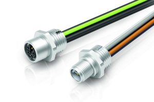
Power supply components intended for control cabinets on the North American continent must meet the specifications of the UL 2237 standard. Engineers at binder have designed panel mount parts with K and L coding as part of the M12 series 824 and 823, which comprehensively follow these requirements.

binder, a leading supplier of industrial circular connectors, offers K- and L-coded panel mount parts within its 824/823 product series, which are intended for power applications in the North American market in compliance with the UL 2237 standard. These include 5-pin male and female panel mount parts featuring screw locking that meet the protection degree criteria of IP68. Electrical and plant engineering as well as industrial controls are the main application areas for these M12 components.

UL 2237 – panel mount parts for North America

The use of electromechanical interfaces for voltage and power transmission in control cabinets of the North American applications market requires approvals according to UL 2237. This standard specifies testing guidelines for connectors, cables, cable glands, and fuse elements, such as the Grounding (Bonding) Path Current Test: this procedure stipulates the PE path (protection earth) to withstand a current of 190 A for the wire gauge AWG16 or 300 A in the case of AWG14 for four seconds without interrupting. AC applications also require an abnormal-overload test to be carried out at 1.5 times the rated current – where the PE path fuse must not blow – as well as an additional connection of the PE pin to the component housing.

Panel mount parts featuring K and L coding

According to the DIN EN 61076-2-111 standard, K coding indicates 5-pin M12 connectors for power supply to AC applications such as drives or frequency converters. The rated voltage and current limits are specified at 630 V(AC) and 12 A, respectively. The L coding also refers to a 5-pole mating face but is particularly designed for DC applications up to 63 V(DC) and 16 A. These include, for example, smaller motors or fieldbus devices in the industrial-automation sector.

824 and 823 panel mount parts at a glance

The 5-pin panel mount parts of the binder 824 and 823 series with K coding (pin count 4+PE) and with L coding (pin count 4+FE, functional earth) feature M12 screw locking. The termination types are single wires. Both the K- and L-coded components were designed for wire gauges AWG16 and AWG14. For the AC components with K coding, the requirements of UL 2237 were implemented via a PE connection to the threaded ring. UL 2237 approval is currently being prepared.

The mechanical lifespan of the panel mount parts is rated at >100 mating cycles. The temperature limits are -40/+85 °C (Series 824) and -40/+105 °C (Series 823).

Farnell empowers engineers with Superior Sensor Technology’s cutting-edge pressure sensors

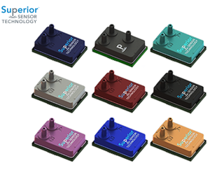
Farnell has announced a distribution agreement with Superior Sensor Technology, a pioneer in application-specific pressure sensors for the medical, industrial, and HVAC markets.

Engineers are often faced with the challenge of finding customisable pressure sensor systems for their specific applications. Traditional sensors require significant time and effort for customisation, which can sometimes lead to project delays.

Superior Sensor’s products are based on their proprietary NimbleSense architecture that turns the pressure sensor into a fully integrated module that combines a MEMS sensor with additional circuitry and software. Superior Sensor’s NimbleSense architecture delivers fully integrated solutions with application-specific capabilities, making it a more efficient and cost-effective option for engineers.

Anthony Gioeli, Vice President of Marketing at Superior Sensor Technology said: “We are proud to offer engineers pressure sensors with a modular architecture providing unique features based on the end application. Our core technology has an impressively low noise floor, ensuring higher accuracy. With our ability to integrate advanced functionality like closed loop control, pressure switch, notch filter, and advanced digital filtering, our sensors eliminate the need for external designs.

“Customers can also take advantage of programmable features like bandwidth filtering and variable pressure ranges allowing our customers to further optimise their pressure sensors.”

Superior Sensor Technology provides a range of application-specific pressure sensors for various industries, including HVAC, industrial use cases, medical ventilators, CPAP machines for sleep apnea, spirometers, and UAVs.

Superior Sensors products are now in stock at Farnell in EMEA, Newark in North America and element14 in APAC.

Mouser Electronics empowers innovators with practical guidance for accelerated IoT application development

Mouser Electronics, Inc., the industry’s leading New Product Introduction (NPI) distributor with the widest selection of semiconductors and electronic components™, will be organizing a free workshop to help engineers developing IoT applications to accelerate their projects with secure IoT cloud deployment. Mouser has partnered with Würth Elektronik to hold a limited-space “Build A Secure Rapid IoT Application Connected To Microsoft Azure Cloud” workshop, which will take place in Munich on 8 November.

“IoT innovation is playing an active role in shaping today’s businesses and consumer trends, and Mouser is continuously working with leading suppliers to support design engineers from prototyping to production,” says Mark Patrick, Director Technical Content, EMEA at Mouser Electronics. “With this workshop, we are offering hands-on experience with the latest tools and technologies to help innovators jumpstart their IoT projects confidently.”

Participants attending the workshop will gain the skills to create a rapid end-to-end IoT solution with secure cloud connectivity to Microsoft Azure to empower IoT data utilisation. Attendees will receive practical advice from three experts in IoT hardware development, wireless connectivity, and secure IoT cloud deployment. Guest speakers include Rafik Mitry, Technical Marketing Engineer at Mouser Electronics, Adithya Madanahalli, IoT Engineer at Würth Elektronik eiSos and Chris Jones, Director of Applications at Crypto Quantique.

The speakers will demonstrate how IoT project development can be accelerated using the Calypso IoT design kit from Würth Elektronik. Participants will be provided with one of these powerful IoT design kits to use during the workshop and will be able to keep it as their own resource, giving them all the necessary tools and components for secure IoT development in the future.

The Calypso IoT design kit, available to order from Mouser, is ideal for prototyping sensor-to-cloud IoT applications, allowing the user to monitor temperature, absolute pressure, relative humidity and 3-axis acceleration. The Adafruit Feather-based board features the M0 Feather stacked with Calypso Wi-Fi FeatherWing, the Sensor FeatherWing, and the OLED FeatherWing. The kit also offers plug-and-play secure connectivity to Azure IoT Central.

As the workshop is a live event, attendance is limited to 50 participants. To register and find out more, visit: https://emea.info.mouser.com/wuerth-iotcloud-workshop/.

Siemens’ company Enlighted adds powerful new AI capabilities for IoT in buildings

Enlighted, a leading property technology company owned by Siemens, has announced the expanded use of artificial intelligence (AI) in its Location Services solution, and the addition of two new partners to the Enlighted AI partner ecosystem.

Enlighted’s Location Services – a Real Time Location System (RTLS) – tracks the location and movement of assets and badges in buildings, using existing Enlighted intelligent lighting infrastructures. With the introduction of AI machine-learning models, the accuracy of finding assets and personnel badges is improved to greater than 98 percent, empowering businesses across industries to optimize their operations and better control inventory.

High levels of accuracy are especially critical in healthcare and manufacturing, where understanding exact location is essential for many critical use cases. The enhanced system reduces implementation costs dramatically via existing Bluetooth-enabled lighting control sensors. These AI capabilities build on the existing Enlighted Touchless Workplace solution, an AI-driven mobile app which allows occupants to control workplace temperature.

AI solutions Location Services (RTLS) and Touchless Workplace are part of the Siemens Xcelerator Marketplace, an open digital business platform to accelerate digital transformation.

“Sensors in smart buildings collect an enormous amount of data. AI-based applications are a transformative way for commercial buildings to maximize and use this data, optimizing efficiency while improving the occupant experience,” said Stefan Schwab, CEO of Enlighted. “These new capabilities and partnerships demonstrate that Enlighted is continuously innovating and expanding its offerings with the most advanced technology.”

The Addition of Two New AI Partners

Enlighted has also expanded its partner ecosystem with participants who bring AI applications, machine-learning tools and platforms that extend the value from vast volumes of Enlighted time-series IoT building data.
  • Tagnos, a healthcare solution provider, is leveraging Enlighted’s AI generated RTLS location data as part of its Healthcare Orchestration Platform, to drive patient care and asset tracking workflows in hospitals.
  • Zan Compute, a smart building systems provider, is using Enlighted’s occupancy data and their own AI analytics to guide necessary cleaning activity, reducing building cleaning costs, and improving occupant experience.

DigiKey launches Season 1 of MedTech Beyond video series

DigiKey, a leading global commerce distributor offering the largest selection of technical components and automation products in stock for immediate shipment, announced the launch of its new MedTech Beyond video series.

Sponsored by NXP® Semiconductors and RECOM Power, the three-part video series dives into how medical devices are evolving and allowing for faster and more accurate diagnosis and treatment. From wearables to immersive tech and AI-powered innovations, the series explores how medical technology is creating opportunities to live longer, more fulfilling lives.

“As healthcare needs and technology both rapidly advance, DigiKey is proud to support the needed technology advancements,” said Josh Mickolio, supplier business development manager – wireless and IoT for DigiKey. “Medtech advancements are enhancing every aspect of healthcare and ultimately leading to longer, more fulfilling lives.”

“Our power supplies play a pivotal role in enabling cutting-edge medical devices to operate flawlessly, ensuring precision and reliability,” said Chris Wolf, president, RECOM Power. “At RECOM, we take pride in contributing to the advancement of medical technology, and we remain dedicated to powering a healthier and more connected world.”

“An important change in the medtech landscape is the ‘scale’ of care, as we see an increased need to manage healthcare in the home,” said Luca Difalco, senior vice president, global sales offerings for NXP Semiconductors. “Our technology enables the democratization of health monitoring and diagnostics while helping to ensure the security of the data and device. The ability to offer advanced quality, long product lifecycles and a wide portfolio of offerings positions NXP well to help advance the medtech industry.”

The first of three videos in the series, “Holistic Health,” is now live on DigiKey’s website, and investigates the evolution of tech-assisted personal wellness and patient care. Personal wellness tech is no longer limited to counting steps. A new generation of patient care and personalized medical devices are using the latest technology to provide a better patient experience and a more holistic look at daily health.

The second video, “Engineering Better Health Outcomes,” explores how innovation happens behind the scenes with industry leaders. Given the critical importance of patient safety and security, medical device engineers, designers and supply chains face more pressure than most.

The third and final video in the first season of the series, “Curing Tomorrow,” examines the big thinkers investigating the next medtech breakthrough. From AI-powered diagnostics to predictive analytics, investigate how today’s innovations are helping diagnose and treat the diseases of tomorrow.

To learn more about the video series and how DigiKey is supporting the rapidly evolving medtech sector, visit the DigiKey website.

Farnell and Tektronix collaborate to bring a new video series on NXP LPCXpresso55S69 development board to the engineers

Farnell is hosting a video series by Tektronix taking a deep dive into one of the most popular development boards from NXP, the LPCXpresso55S69.

The LPCXpresso55S69 is a powerful development board with an MCU based on the Arm Cortex M33 architecture. It features UART and SPI support, an audio subsystem, a built-in accelerometer, and a host of connectivity options providing expansion for your embedded projects.

Developed by Tektronix, the video series will explore the various signals that are typically measured during the development of electronic projects with a focus on the embedded, power and automotive sectors.

Across six episodes, the short films will provide insights on the latest test and measurement solutions, such as oscilloscopes, probing solutions, fast sampling high-resolution digital multimeters, source measuring units, and arbitrary function generators, to help viewers understand how to measure these signals effectively. In addition, a range of topics are covered including:

  • Power consumption
  • Power Rail noise and ripple
  • Serial decode and trigger on a variety of buses
  • Analyzing potential EMI
  • Clock and signal integrity
  • Audio sub-system performance

Lee Turner, Vice President, Product and Supplier Management at Farnell Global, said:  “We are thrilled to partner with Tektronix to offer this video series on the LPCXpresso55S69 development board. Through this, customers can learn from one of the industry’s leading experts about the features and capabilities of this powerful development board, as well as how to use the latest test and measurement solutions to analyse and optimise their designs.”

This video series is a must-watch for anyone interested in embedded systems development and testing. Check out the first two episodes at https://uk.farnell.com/tek-nxp-application?ICID=I-HP-LB-TEKTRONIX-NXP-APPLICATION-AUG-FY23-WF3358595, and please bookmark this page to be notified of the latest episode so you don’t miss out.

ABB and Imperial College extend carbon capture collaboration to support future workforce and energy transition

A dedicated carbon capture pilot plant will continue to train the net-zero workforce, and engineers and scientists of the future, after ABB and Imperial College London signed a 10-year contract to extend their successful partnership. The plant is the only one of its kind in an academic institution in the world.

More than 4,500 students have had hands-on experience of ABB’s technology solutions at the plant since it opened in 2012 at Imperial College, which is one of the world’s top ten universities with a reputation for excellence in science and engineering.

With the agreement, ABB aims to equip today’s students with the skills needed to run tomorrow’s industrial processes by demonstrating how the latest technology can help to optimize plant performance and safely manage emergency situations in real-life applications. The collaboration between ABB and Imperial College gives the university access to some of the most advanced control and instrumentation technology available from any manufacturer.

“Extending the partnership with Imperial College allows us to offer students practical training to prepare them for a career in industry,” said Simon Wynne, Head of Energy Industries, ABB UK & Ireland. “A report by EngineeringUK says that for the UK to meet emissions targets by 2050, there needs to be a workforce, with the right STEM backgrounds, ready to respond to the energy transition challenge.”

The plant, which is spread over four floors, uses ABB Ability™ System 800xA® for distributed process control and over 250 instruments, measuring temperature, pressure, carbon dioxide and flow. System 800xA automatically controls and coordinates all aspects of the plant process, which is then visualized on displays in the ABB Control Room where students can monitor and intervene if necessary.

ABB’s Ability™ Verification for measurement devices and new Ability™ SmartMaster verification and condition monitoring platform are also being used to equip students with the skills needed to optimize instrument performance through predictive maintenance.

“When we started the partnership with ABB, the aim was to encourage more people to go into and stay in chemical engineering,” said Dr Colin Hale, Senior Teaching Fellow at Imperial College London. “One of the ways to do this was to set up this carbon capture plant so we could enthuse students to follow through on the environmental topics they have learnt previously. ABB shares this collective vision.”

“During my time in the carbon capture pilot plant, I have actively participated in the operation of the process, gaining a deeper understanding of the development and application of the technology,” said Yiheng Shao, fourth year undergraduate student at Imperial College London. “This experience has also bolstered my confidence in the role of carbon capture in achieving net-zero goals.”

According to a report by S&P Global, carbon capture and storage (CCS) can help decarbonize industry, reduce emissions and reach net zero, while the Global CCS Institute says in 2022 there was a 44 percent increase in the number of CCS facilities around the world compared with the previous year.

To enable the commercial CCS market to scale, ABB is deploying technology solutions to lower the capital and operational investment costs and de-risk integration into existing and new operations. In March 2023 ABB joined forces with London-based Pace CCS to make the capture, transportation and storage of industrial carbon dioxide emissions more accessible. Key to this is using digital twin technology to provide a virtual replica of a real process to test scenarios and deliver proof of concept.

Earlier this year, the UK Government outlined its Powering Up Britain policy. This series of net-zero pledges, including £20 billion of funding to unlock private investment and jobs in CCS, aims to deliver an energy system with cleaner, more affordable energy sources.