21st November 2019NewsComments Off on Engineers Without Borders UK launches Engineering for People Design Challenge 2020577
Engineers Without Borders UK, part of an international movement putting global responsibility at the heart of engineering, has launched the 2020 cycle of the award-winning Engineering for People Design Challenge in partnership with Engineers Without Borders South Africa and Engineers Without Borders USA.
The unique competition engages first and second-year university students to consider the social, economic and environmental impact of their engineering by inviting them to propose a solution that could be applied to a real-life problem affecting people on a global scale.
Now in its ninth year, the Challenge has reached over 34,500 undergraduate students to date. Already embedded in the undergraduate curriculum at dozens of UK universities, the 2020 instalment has been extended to more than 7,000 students over three continents – with time remaining for more students to get involved.
The 2020 Challenge focuses on Makers Valley, a suburb of Johannesburg, South Africa. As a result of rapid population growth and economic inequality, the area is facing housing shortages, inconsistent access to electricity and water and problems with waste collection.
To overcome these challenges, the residents of Makers Valley have collectively begun working toward urban renewal through creative solutions, empowerment, and collaboration. Students are now invited to join them by designing a potential solution that addresses one of the key issues and is an appropriate fit for the economic, environmental and social context of the community.
Academics from each institution will review their students’ submissions with the top five from each university going forward to be judged by industry volunteers. The best team from each participating university will then be invited to present their solutions at the Grand Finals in London in a bid to win the Grand Prize of a £2,000 educational bursary. The runner-up and the People’s Prize winners will also receive £500 each to share between them.
Emma Crichton, Head of Engineering at Engineers Without Borders UK, said: “Our real-life design project provides a platform for students to truly understand how to develop engineering skills with a globally responsible mindset and place people at the heart of their designs. We are thrilled that our award-winning Engineering for People Design Challenge is reaching a wider audience with students participating from South Africa, UK, Ireland, UAE and the USA. We have already visited half of the currently participating universities, meeting thousands of students around the world. The perspective they bring is invaluable to understanding how we need to continue to improve engineering education to serve the needs of all people and our planet.
“We look forward to welcoming even more students onto the Challenge and sharing their passion for ensuring that every person globally enjoys the same right to dignified living conditions.”
20th November 2019NewsComments Off on RS Components launches DesignSpark membership referral programme with prize incentives576
RS Components (RS) has introduced a referral programme that incentivises members of DesignSpark to introduce friends and colleagues to the leading engineering platform, which offers benefits such as access to a global community of engineers, free MCAD and ECAD design software, CAD neutral libraries and a host of other resources. As the result of a referral, both the existing and newly registered member is entered into a quarterly prize draw, with a chance to win a Fitbit tracker plus £500 of products stocked by RS.
Entry into the draw is automatic for anyone who registers for DesignSpark membership adding the username of an existing member when prompted during the registration process. There are no limitations on the number of referrals, which means the odds of winning are increased for multiple referrals by existing members. What’s more, following a successful registration, each new member then also qualifies to refer a friend or colleague through the programme. As an extra bonus, the top referring DesignSpark member, who has the highest number of new members quoting their username each quarter, will win an exclusive DesignSpark goody bag.
With more than 850,000 members already signed up to the go-to design engineering platform, DesignSpark is the place to discover the latest products and technologies from world leading brands. It is a thriving forum for engineers, enabling meaningful connections with fellow engineers around the world in a rapidly developing environment, as well as access to a range of professional tools and software that help shorten design time and advance productivity.
Natalie Reigel, Head of the DesignSpark Community at RS, said: There’s strength in numbers, and the more members we have in our community, the wider our collective knowledge base and the faster we can support and advise one another. We want to grow our community – spreading the DesignSpark love far and wide – and continue to strengthen our suite of tools and assets for all of our members.”
The first draw will take place on Monday 13 January 2020, for all referrals made between 4 October 2019 and 12 January 2020.
20th November 2019News, Sensors and TransducersComments Off on Mouser Electronics and Amphenol SSI sign global distribution agreement664
Mouser Electronics has announced a global distribution agreement with Amphenol SSI, a leading designer and manufacturer of sensors and sensing solutions for the global automotive and industrial markets. Through the agreement, Mouser now stocks a broad line of Amphenol SSI products, including pressure sensors and gauges, drum liquid level gauges, and combination temperature and pressure gauges.
Amphenol SSI P51 Pressure MediaSensor and P61 Pressure and Temperature MediaSensor families are micro-machined sensors suitable for measuring both harsh and benign media in a variety of automotive, industrial, and commercial applications with superior accuracy. The P51 family devices are available in absolute, vented gauge, or sealed gauge conventions, and measure pressures from 3 PSI to 7500 PSI. The P61 family transducers and transmitters are available in absolute and sealed gauge configurations, and measure pressures from 100 PSI to 3,000 PSI.
The MediaGauge family are three standalone battery-operated digital pressure gauges, each containing a piezoresistive pressure sensing element, signal conditioning for temperature and calibration, a stainless steel input port, and a four-digit display. MediaGauge devices offer a range of accuracies, media isolation, user functions, and output capabilities ideal for applications such as refrigeration, process control, fuel cells, pumps, hydraulics, pneumatics, compressors, and agriculture.
Digital Fluid-Trac devices are noncontact continuous drum liquid level gauges based on ultrasonic technology. The gauges include an LCD display (with 4-20 mA output available) and are designed for use on standard 13-, 30-, and 55-gallon vertical drums storing a wide variety of media such as water, wastewater, motor oil, hydraulic fluid, and diesel fuel.
20th November 2019News, Sensors and TransducersComments Off on Horizon2020-supported Highly Integrated Optical Sensors project successfully completed577
ams, a leading worldwide supplier of high performance sensor solutions and coordinator of the Highly Integrated Optical Sensors (HIOS) consortium, has announced the successful completion of this project. Funded EUR 3 million under the Horizon2020 Grant Agreement nr. 720531 (Fast Track to Innovation), the EUR 4.3 million HIOS project enables ams and its consortium partners, the process and equipment suppliers APC, Boschman and Bühler, to stay at the forefront of sensor integration and drive competitiveness in their respective markets.
Verena Vescoli, Senior Vice President R&D at ams, said: “Thanks to Horizon2020 funding from the European Union and superb collaboration from all partners in the HIOS Consortium, we’ve been able to drive market innovation at a far faster rate than would have otherwise been possible. This is a great example of how European companies can work together to compete on the world stage supported by the European Union.”
Sensors, sensors everywhere!
From personal mobile device to wearables smart homes, offices, cars, and more, people are surrounded by sensors. Sensor functionality is evolving rapidly, from making our phones more intuitive and lighting solutions more intelligent to conserving battery power and enabling breakthrough medical technologies. Sensors therefore play a key role in many applications in markets including mobile and consumer, automotive, and industrial. One thing is constant across these fields: the challenging demand for high performance, such as high sensitivity or low power consumption, often in combination with small size and low cost. However, this drives the need for sensor integration with electronics and other system components which can be highly complex to achieve.
The Highly Integrated Optoelectronic Sensor Consortium
The HIOS Consortium addressed this need for collaborative innovation in the growing market for intelligent light sensors. In particular, HIOS developed and launched the world’s first light sensor with fully integrated optical stack including multiple filters and an aperture replacing multiple discrete components. The sensor in 3D technology, IC filter and Wafer Level Optics integration technology developed in the HIOS project is also expected to bring further cost-efficient, very small, and high-performance sensors to the market. ams established a high-volume production environment for 3D/Through Silicon Via (TSV) process technology which has now been extended by equipment and processes for on-chip inorganic optical filters and wafer level molding to form on-chip optical components.
Leading in optical sensor products
HIOS’ ambitious goal was to develop an industry-leading class of new optical sensor products offering the highest possible integration of components and miniaturization. Departing from the initial concept for an Ambient Light Sensor, the project focused on enabling the later launch of a color sensor as an achievable target. To reach this shared goal, all partners had to push the boundaries of capabilities in their fields while cooperating seamlessly at the same time.
Bühler developed and enhanced new equipment for advanced optical interference filter processing and announced its new deposition tool for high performance optical coating, HELIOS Gen II, in February 2019. This is the latest version of its highly-successful sputter tool with improved layer distribution and enhanced low particle process. New hardware and PARMS+ process lead to a tighter specification with high productivity and yield. Boschman successfully established a new level of accuracy with its molding tool and process development for optical packaging applications being capable to form diffusor layers, lenses and apertures.
Innovation successfully demonstrated
As planned, all these developments were successfully demonstrated for implementation on the ams family of ambient light sensors products. Based on the excellent quality of the interference filters developed throughout this project, new spectral color sensor products could be designed covering applications from UV, visible and infrared wavelengths.
In 2018, a first color sensing product was launched delivering the first engineering samples for a miniaturized 18 channel (3×6) spectral sensor family (AS7265x).
Given high interest in these new highly-integrated sensing applications, ams successfully launched the AS7341 color sensor, an 11-channel spectrometer for spectral identification and color matching applications, in January 2019. With 8 optical channels, this sensor enables new spectral sensing functions for mobile devices covering the whole visible range from UV to near infrared. With an additional 3 extra channels for Clear, NIR and Flicker it also allows exact determination of 50Hz or 60Hz ambient light flicker to minimize distortion of ambient light sources.
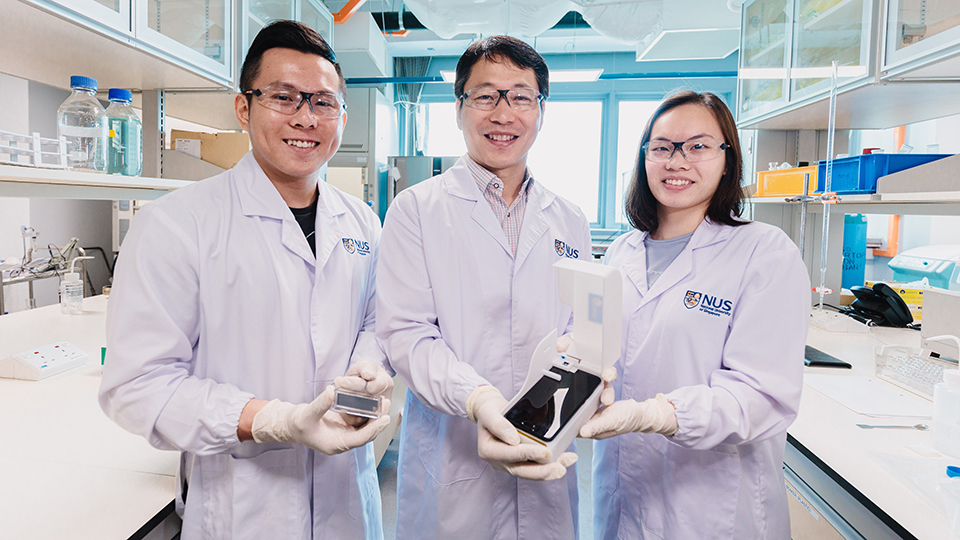
A team of engineers from NUS has developed a highly sensitive system that uses a smartphone to rapidly detect the presence of toxin-producing algae in water within 15 minutes. This invention can generate test results on-site, and findings can be reported in real-time using the smartphone’s wireless communications capabilities.
The NUS research team behind the novel algae detection device is led by Assistant Professor Bae Sung Woo (centre) who is holding the smartphone platform. With him are two team members: Mr Thio Si Kuan (left) who is holding the microfluidic chip, and Miss Chiang Li Ching Elaine (right)
This technological breakthrough could play a big role in preventing the spread of harmful microorganisms in aquatic environments, which could threaten global public health and cause environmental problems.
The NUS team, led by Assistant Professor Bae Sung Woo from NUS Civil and Environmental Engineering, first published the results online in scientific journal Harmful Algae on 25 July.
Current challenges of water quality monitoring
A sudden surge in the volume of algae and their associated toxins in lakes, ponds, rivers, and coastal waters can adversely affect water quality, and in turn, may have unfavourable effects on human health, aquatic ecosystems, and water supply. For instance, in 2015, an algae bloom wiped out more than 500 tonnes of fish in Singapore, and caused some fish farmers to lose millions of dollars.
Conventional methods of algae detection and analysis are time consuming, and require specialised and costly equipment, as well as skilled operators to conduct water sampling and testing. One approach is to test for the presence of chlorophyll using complex instruments that cost more than S$3,000 (US$2,200). Another common method is to carry out cytometric and image analysis to detect algal cells – this method involves equipment that cost more than S$100,000 (US$73,000).
“Currently, it can take a day or more to collect water samples from a site, bring them back to the laboratory for testing, and analyse the results. This long lead time is impractical for monitoring of algae blooms, as the management of contamination sources and affected waters could be slowed down,” explained Asst Prof Bae.
To address the current challenges in water quality monitoring, Asst Prof Bae and his team took a year to develop the novel device that monitors microbial water quality rapidly and with high reliability.
New ‘lab-on-a-chip’ technology: Cheaper, smaller and highly sensitive
The new NUS invention comprises three sections – a microfluidic chip, a smartphone, and a customisable 3D-printed platform that houses optical and electrical components such as a portable power source and an LED light.
The chip is first coated with titanium oxide phthalocyanine, a type of photoconductive polymer-based material. The photoconductive layer plays the important role of guiding water droplets to move along the chip during the analysis process.
The coated chip is then placed on top of the screen of a smartphone, which projects a pattern of light and dark regions onto the chip. When droplets of the water sample are deposited on the surface of the chip, a voltage drop difference, created by the light and dark areas illuminated on the photoconductive layer, modifies the surface tension of the water droplets. This causes the water droplets to move towards the dark illuminated areas. At the same time, this movement induces the water droplets to mix with a chemical that stains algae cells present in the water sample. The mixture is guided by the light patterns towards the camera of the smartphone.
Next, an LED light source and a green filter embedded in the 3D-printed platform, near the camera of the smartphone, create the conditions suitable for the camera to capture fluorescent images of the stained algae cells. The images can be sent to an app on the smartphone to count the number of algae cells present in the sample. The images can also be sent wirelessly to another location via the smartphone to quantify the number of algae cells. The entire analysis process can be completed within 15 minutes.
This portable and easy-to-use device costs less than S$300 (US$220) – excluding the smartphone – and weighs less than 600 grams. The test kit is also highly sensitive, hence only a small amount of water sample is needed to generate reliable results.
The smartphone device can generate test results on-site, and findings can be reported in real-time
High detection accuracy of 90 per cent
The NUS research team tested their system using water samples collected from the sea and reservoirs. The water samples were filtrated and spiked with specific amounts of four different types of toxin-producing algae – two types of freshwater algae C. reinhardtii and M. aeruginosa, and two types of marine water algae Amphiprora sp and C. closterium. Experiments using the new device and a hemocytometer, a standard cell-counting technique commonly used for water quality monitoring, were conducted to test for the presence of algae.
The new smartphone system was able to detect the four types of algae with an accuracy of 90 per cent, comparable with the results generated by the hemocytometer.
Asst Prof Bae shared, “The combination of on-chip sample preparation, data capture and analysis makes our system unique. With this tool, water quality tests can be conducted anytime and anywhere. This new method is also very cost efficient as the microfluidic chip can be washed and re-used. This device will be particularly useful for fish farmers who need to monitor the water quality of their fish ponds on a daily basis.”
This project was supported by the National Research Foundation Singapore through its Marine Science Research and Development Programme, and the Ministry of Education.
Commercialisation and further studies
The research team is currently in discussion with industry partners to commercialise their technology.
The NUS researchers are also developing a new microfluidic chip that can be integrated with a modified version of the current 3D-printed smartphone platform to detect the presence of foodborne pathogens such as salmonella and other infectious pathogens.
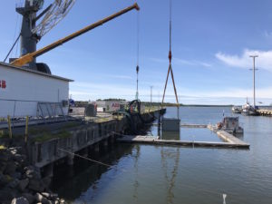
ABB’s pioneering subsea power distribution and conversion technology system is commercially viable, bringing groundbreaking potential for cleaner, safer and more sustainable offshore oil and gas production, following the completion of a 3,000-hour shallow water test.
For the first time worldwide, energy companies will be able to access a reliable supply of up to 100 megawatts of power, over distances up to 600 kilometers and down to 3,000 meters water depth, at pressures that could shatter a brick. This is all achievable with a single cable with little or no maintenance for up to 30 years, making oil and gas production feasible in far out and deep ocean environments.
The $100 million research, design and development Joint Industry Project (JIP) between ABB and Equinor with its partners Total and Chevron was initiated in 2013. The validation of the shallow water test at a sheltered harbor in Vaasa, Finland, means the majority of the world’s offshore hydrocarbon resources are now in reach for electrification.
“This milestone marks an outstanding achievement and is the culmination point of an inspirational technology development achieved through tremendous dedication, expertise and perseverance. It is the result of intensive collaboration by over 200 scientists and engineers from ABB, Equinor, Total and Chevron in a multi-year, joint effort,” said Dr. Peter Terwiesch, President of ABB’s Industrial Automation business.
By powering pumps and compressors on the seabed, closer to the reservoir, ABB’s subsea power distribution and conversion technology can significantly reduce power consumption. There is potential for substantial energy savings, with reduced carbon emissions using power from shore. ABB’s subsea power technology can connect to any power source, enabling future integrations with renewable energy, such as wind and hydro power.
Based on a specific field development case, the new technology could offer CAPEX savings of more than $500 million, if eight consumers, such as pumps or compressors, are linked through a single cable over a distance of 200 km from other infrastructure.
Having fewer people offshore will reduce risks and improve overall safety. Against a backdrop of digitalization and increasing autonomy in offshore operations, new opportunities are also anticipated in the ocean ecosystem.
“Moving the entire oil and gas production facility to the seabed is no longer a dream. Remotely operated, increasingly autonomous, subsea facilities powered by lower carbon energy are more likely to become a reality as we transition towards a new energy future,” said Dr. Terwiesch.
Previously, only the transmission cable and subsea step-down transformer were proven to operate underwater. Today, ABB’s complete subsea power distribution and conversion system includes a step-down transformer, medium voltage variable speed drives and switchgear, control and low voltage power distribution, and power electronics and control systems. ABB’s flagship distributed control system, ABB Ability System 800xA, controlled the rigorous testing.
20th November 2019News, Test and MeasurementComments Off on Vision Engineering celebrates Mantis microscope success with 20,000 sales in five years760
Vision Engineering, a leading manufacturer of high-quality visual inspection and measurement technologies, has sold over 20,000 Mantis microscope products in the last five years.
The Mantis range of ergonomic eyepiece-less stereo microscopes offers superb optical performance with magnification options up to 20x, making it a perfect alternative to more traditional inspection stereo microscopes.
The Mantis, introduced in 1994, was the world’s first ‘eyepiece-less’ stereo microscope – its high-performance capabilities which focused on operator comfort soon became Vision Engineering’s best-selling product. Since then, Vision Engineering has continued to pursue a corporate design and innovation policy that concentrates on optimising operator performance when using optical systems in the manufacturing sectors and industries.
Mantis is still Vision Engineering’s most successful and popular product-range, offering Mantis Compact, Mantis Elite, and Mantis Elite-Cam HD to aid workers in production, quality control and rework environments. The clarity, user-comfort and optical performance of a Mantis microscope has saved manufacturing companies many man-hours, reduced materials wastage and ensured quality and conformance to desired specifications.
Mantis has also shown its star potential appearing in countless news articles and in films, having been presented alongside actors such as Ben Affleck, Uma Thurman and Jim Carrey.
Mark Curtis, Managing Director, Vision Engineering comments: “We are thrilled to see the continued success of Mantis – even after so many years, it’s clear that many workers in the manufacturing industry require the combination of precision and comfort which is simply not attainable with any other microscope range on the market.
“The popularity of one of our leading products is a testament to the power and clarity of our eyepiece-less microscope. This confirms that workers manufacture better quality materials, components and equipment whilst simultaneously speeding up processes and improving workplace efficiency.”
19th November 2019NewsComments Off on The hunt is on for the engineers of the future667
The Oxfordshire Advanced Skills training centre is on the hunt for more than 100 engineers of the future to fill apprenticeship places.
The apprentices will be part of September 2020’s intake, and will start their training at the newly opened 3,800 sq metre training academy at the UK Atomic Energy Authority’s site at Culham Science Centre near Abingdon.
An open evening to showcase the training facilities will be held at the new centre on Thursday 28 November from 5pm to 7pm. The event will give visitors the opportunity to learn about the apprenticeships, and also understand the needs of some of the employers with whom the centre is currently working. Anyone interested should register at https://www.oas.ukaea.uk/open-evenings/
The Coventry-based Advanced Manufacturing Training Centre (AMTC) teamed up with the UKAEA and the Science and Technology Facilities Council to train hundreds of apprentices in the new academy.
UKAEA has partnered with STFC to form OAS to increase the amount of trained technicians available to local employers in the county – one of the UK’s high-tech hotspots. More than 100 apprentices will begin next September, with a further 100 being recruited at the Advanced Manufacturing Training Centre in Coventry.
Training at the new facility is being delivered by the AMTC, replicating the industry-leading training centre in Coventry. The AMTC has built a rapid reputation for equipping apprentices not only with core engineering skills but also the latest advanced manufacturing techniques.
The Abingdon centre will be equipped with industry-standard equipment covering a wide range of engineering and technology disciplines.
Paul Rowlett, Managing Director of the Advanced Manufacturing Training Centre, said: “Having an insight into tomorrow’s technology gives us the ability to create training programmes and apprenticeships to equip industry with a capable workforce. We are delighted to be working with UKAEA and STFC to deliver the Oxfordshire Advanced Skills training programme. There is a clear synergy and shared vision across our organisations.”
Anyone interested in more information on OAS apprenticeships should visit https://www.oas.ukaea.uk
18th November 2019NewsComments Off on Innovation hub to accelerate scientific breakthroughs647
A new EU innovation hub – ACTPHAST 4R – specialising in the deployment of cutting-edge photonics technologies will give researchers in academic institutes all over Europe the chance to turn their breakthrough scientific concepts into industrially-relevant demonstrators.
Launched this year, ACTPHAST 4R (short for ‘ACTPHAST for Researchers’) has financial support from the European Commission under the H2020 Framework, to solve the bottleneck in developing a concept into a prototype.
Centrally coordinated by the Brussels Photonics Team (B-PHOT) at the Vrije Universiteit Brussel, ACTPHAST 4R will support 800 researchers from across Europe over the next four years.
Providing them with open access to expert coaching in the accelerated development and deployment of photonics from its panel of 200 top photonics experts, ACTPHAST 4R expects to select at least 100 of the researchers to receive further deep innovation project support to build their demonstrators.
An extension of ACTPHAST 4.0, the existing EU photonics innovation incubator for SMEs, ACTPHAST 4R is set to be a game-changer in the European innovation ecosystem. For the first time, researchers will have access to support to progress seamlessly from early-stage breakthroughs right through to advanced prototypes and into industrial use.
With 24 of Europe’s top photonics competence centres, ACTPHAST 4R will make advanced photonics resources available to all researchers on an open-access one-stop-shop basis.
Photonics Technologies
Photonics – the science behind the power of light – is a critical digital technology for the creation of new applications and solutions that address many of our major societal challenges from Optical Communications and High-Performance Computing, to Environmental Sustainability, Industry 4.0, Smart Living and Personalised Healthcare.
While researchers working in different scientific domains behind these applications often have breakthrough concepts, many lack the expertise in photonics and easy access to the advanced photonics technology platforms in order to develop fully-functioning industrially-relevant demonstrators.
Significantly, ACTPHAST 4R’s deep innovation support will involve internships and hands-on training for the researchers in the state-of-art technology platforms and equipment of the host competence centres.
Researchers will get access to intensive entrepreneurial coaching, ensuring a durable knowledge transfer and cross-fertilisation of photonics with other key scientific domains with a focus on commercial deployment.
Ambitious Impact Targets
Over the next 4 years, ACTPHATS4R expects to create 50 high-tech jobs in new spin-out companies (creating new positions like CEOs, CTOs and Heads of Innovation, Engineering and Product Development).
As a result of its support activities with European researchers, the innovation hub will foster 30 new IP depots, patent applications or strengthened patents, 20 new IP transfer or technology licensing agreements with industry, and help to generate €15M in new venture capital.
Project coordinator and managing director of the Brussels Photonics Team at VUB, Professor Hugo Thienpont said: “The ambitious ACTPHAST 4R programme will greatly strengthen the European innovation ecosystem.”
“We will open up access to advanced prototyping platforms for researchers and tackle critical roadblocks at the early stage TRL levels in the bridge between fundamental and applied research.
“Through this facility, we will create new opportunities to deliver advanced photonics technologies and sustainable growth across all European regions,” Professor Thienpont said.
Catering to photonics and non-photonics researchers alike, the new facility will provide a full supply chain of services such as design, measurement and packaging, with transnational internships and expertise from Europe’s leading photonics research institutes.
In parallel, ACTPHAST 4R participants will also get exclusive access to expert coaching in technology deployment and entrepreneurship.
“We offer services that are unique for turning research into real products. All of the ACTPHAST 4R services are made available in a subsidized format for collaborating on photonics innovation projects.
“With an average ‘incubation’ time of 6 months per project, we expect that ACTPHAST 4R will accelerate the development of new applications, enterprises and jobs, and the diffusion of innovation for the betterment of society in Europe and beyond,” said Thienpont.
Unique Innovation Support
The ACTPHAST4R model is unique in a European context in that it is designed to provide a single entry point into a fully integrated “one-stop-shop” supply chain for innovation support across the broad spectrum of photonics technology platforms.
ACTPHAST4R, together with ACTPHAST 4.0 and the European pilot lines in photonics, will complete the essential bridges across the ‘Valley of Death’ between research and development where the flow of innovation is often de-railed, namely:
Demonstration of Conceptual Breakthroughs moving from fundamental research (TRL1-2) to applied research (TRL3-4);
Prototyping moving from applied research (TRL3-4) to advanced prototypes for industrial applications (TRL5-6), and;
Scaling Manufacturability moving from small-scale prototypes (TRL6-7) to mass-market products (TRL8-9).
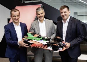
Schaeffler and Audi are set to remain a formidable Formula E team in the future.
This agreement was concluded between the globally active automotive and industrial supplier from Herzogenaurach and the brand from Ingolstadt. Joint development work on the Audi e-tron FE07 for the series’ seventh season, starting out in autumn 2020, has already begun. This is one of the most successful partnerships in Formula E: since the series made its debut in the fall of 2014, Schaeffler has been the technology partner of Audi Sport ABT Schaeffler. The team has set benchmarks both on the track and on the sidelines, with 40 places on the podium and more than 1,000 points before the start of the sixth season. Schaeffler puts the expertise gained from this fully electric racing series into its development work.
Successful partnership in Formula E
“Schaeffler, Audi, and Formula E are a combination that was perfect from the very start,” explains Matthias Zink, CEO Automotive OEM at Schaeffler. “As a company, our intention is to use our drive train and chassis technologies to innovatively shape sustainable mobility. Formula E is an ideal platform on which to present these ideas for future electric mobility and measure our performance in a competition of the highest sporting calibre. And at the same time, our involvement has been delighting both fans and employees alike for years.”
Initially a partner to the private ABT Sportsline team for the first three years, Schaeffler has been developing drive trains for Formula E together with Audi since it joined the series as a factory team in the fall of 2017. The combination of engine, transmission, inverter, and software represents the core of the vehicle, which in all other aspects is identical for all teams. In the future, Schaeffler will continue its involvement as a technology and development partner, primarily in fields such as transmission, engine, and drive concept development and by providing support in test rig-based work and prototype construction, as well as bearing development and production. “I am delighted that the formidable team of Audi and Schaeffler will continue during the next few years,” enthuses Dieter Gass, Audi’s head of motorsport. “We have already achieved a great deal together, but the ever-increasing performance density in Formula E means we still have huge challenges ahead of us. The fact that we are able to join forces and tackle the development of the Audi e-tron FE07 for season seven as an experienced team is therefore of major significance.”
Ideal test laboratory for volume production developments
For Schaeffler, this electric racing series is the ideal test laboratory for developing mobility solutions for tomorrow. After all, only the technology winners in that arena can later hope to be among the leaders in the volume production race. “Formula E gives us a wealth of expertise, which we then transfer from the racetrack to our development departments,” explains Dr. Jochen Schröder, head of Schaeffler’s E-Mobility business division. “The relevance of this expertise in the fields of comprehensive drive systems, electric motors, power electronics, and transmissions is already demonstrated by the Schaeffler electric axle drives that we have been producing for the Audi e-tron since 2018, and this expertise is also being integrated into electric drive systems and components for the future that are currently in volume production development at Schaeffler.”